- 您现在的位置:买卖IC网 > Sheet目录1997 > ICS8430S07AKILF (IDT, Integrated Device Technology Inc)IC CLK GENERATOR PLL 32VFQFN
ICS8430S07AKI REVISION A SEPTEMBER 3, 2009
3
2009 Integrated Device Technology, Inc.
ICS8430S07I Data Sheet
CLOCK GENERATOR FOR CAVIUM PROCESSORS
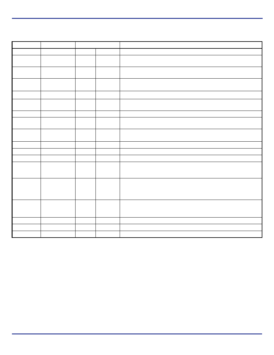
Table 1. Pin Descriptions
NOTE: Pullup and Pulldown refer to internal input resistors. See Table 2, Pin Characteristics, for typical values.
Number
Name
Type
Description
1, 15
VDD
Power
Core supply pins.
2
nPLL_SEL
Input
Pulldown
PLL bypass. When LOW, selects PLL (PLL Enable). When HIGH, bypasses
the PLL. LVCMOS/LVTTL interface levels.
3, 4
XTAL_IN,
XTAL_OUT
Input
Parallel resonant crystal interface. XTAL_OUT is the output, XTAL_IN is the
input.
5
nXTAL_SEL
Input
Pulldown
Selects XTAL inputs when LOW. Selects differential clock (CLK, nCLK) input
when HIGH. LVCMOS/LVTTL interface levels.
6
CLK
Input
Pulldown
Non-inverting differential clock input.
7
nCLK
Input
Pullup/
Pulldown
Inverting differential clock input. Internal resistor bias to VDD/2.
8, 20, 21, 27
GND
Power
Power supply ground.
9, 10
PCI_SEL1,
PCI_SEL0
Input
Pulldown
Selects the PCI/PCI-X reference clock output frequency. See Table 3C.
LVCMOS/LVTTL interface levels.
11, 12
DDR_SEL1,
DDR_SEL0
Input
Pulldown
Selects the DDR reference clock output frequency. See Table 3B.
LVCMOS/LVTTL interface levels.
13, 14
nQA, QA
Output
Differential output pair. LVPECL interface levels.
16
VDDA
Power
Analog supply pin.
17
VDDO_B
Power
Bank B output supply pin. 3.3 V or 2.5V supply.
18, 23, 26,
29, 30,
31
QB, QC, QD,
QREF2, QREF1,
QREF0
Output
Single-ended outputs. LVCMOS/LVTTL interface levels.
19
MR/nOE_REF
Input
Pulldown
Active HIGH Master Reset. Active LOW output enable. When logic HIGH, the
internal dividers are reset and the QREF[2:0] outputs are in high impedance
(HI-Z). When logic LOW, the internal dividers and the outputs are enabled.
LVCMOS/ LVTTL interface levels.
22
CORE_SEL
Input
Pulldown
Selects the processor core clock output frequency. The output frequency is
50MHz when LOW, and 33.333MHz when HIGH. See Table 3A.
LVCMOS/LVTTL interface levels.
24
VDDO_C
Power
Bank C output supply pin. 3.3 V or 2.5V supply.
25
VDDO_D
Power
Bank D output supply pin. 3.3 V or 2.5V supply.
28, 32
VDDO_REF
Power
REF bank output supply pins. 3.3 V or 2.5V supply.
发布紧急采购,3分钟左右您将得到回复。
相关PDF资料
ICS8430S10BYI-02LF
IC CLK GENERATOR PLL 48TQFP
ICS84314AY-02LFT
IC SYNTHESIZER 700MHZ 32-LQFP
ICS843156AKILF
IC CLK GENERATOR 32VFQFP
ICS843156AKLF
IC CLK GENERATOR 32VFQFP
ICS843202AYILF
IC SYNTHESIZER 680MHZ 32-LQFP
ICS843204AGILF
IC SYNTHESIZER LVPECL 48-TSSOP
ICS84320AY-01LN
IC SYNTHESIZER GP LVPECL 32-LQFP
ICS84320AYI-01LF
IC FREQ SYNTHESIZER 32TQFP
相关代理商/技术参数
ICS8430S07AKILFT
功能描述:IC CLK GENERATOR PLL 32VFQFN RoHS:是 类别:集成电路 (IC) >> 时钟/计时 - 专用 系列:- 标准包装:1,500 系列:- 类型:时钟缓冲器/驱动器 PLL:是 主要目的:- 输入:- 输出:- 电路数:- 比率 - 输入:输出:- 差分 - 输入:输出:- 频率 - 最大:- 电源电压:3.3V 工作温度:0°C ~ 70°C 安装类型:表面贴装 封装/外壳:28-SSOP(0.209",5.30mm 宽) 供应商设备封装:28-SSOP 包装:带卷 (TR) 其它名称:93786AFT
ICS8430S07I
制造商:IDT 制造商全称:Integrated Device Technology 功能描述:Clock Generator for Cavium Processors
ICS8430S10AYILF
功能描述:IC CLK GENERATOR PLL 48TQFP RoHS:是 类别:集成电路 (IC) >> 时钟/计时 - 专用 系列:- 标准包装:1,500 系列:- 类型:时钟缓冲器/驱动器 PLL:是 主要目的:- 输入:- 输出:- 电路数:- 比率 - 输入:输出:- 差分 - 输入:输出:- 频率 - 最大:- 电源电压:3.3V 工作温度:0°C ~ 70°C 安装类型:表面贴装 封装/外壳:28-SSOP(0.209",5.30mm 宽) 供应商设备封装:28-SSOP 包装:带卷 (TR) 其它名称:93786AFT
ICS8430S10AYILFT
功能描述:IC CLK GENERATOR PLL 48TQFP RoHS:是 类别:集成电路 (IC) >> 时钟/计时 - 专用 系列:- 标准包装:1,500 系列:- 类型:时钟缓冲器/驱动器 PLL:是 主要目的:- 输入:- 输出:- 电路数:- 比率 - 输入:输出:- 差分 - 输入:输出:- 频率 - 最大:- 电源电压:3.3V 工作温度:0°C ~ 70°C 安装类型:表面贴装 封装/外壳:28-SSOP(0.209",5.30mm 宽) 供应商设备封装:28-SSOP 包装:带卷 (TR) 其它名称:93786AFT
ICS8430S10BYI-02LF
功能描述:IC CLK GENERATOR PLL 48TQFP RoHS:是 类别:集成电路 (IC) >> 时钟/计时 - 专用 系列:- 标准包装:1,500 系列:- 类型:时钟缓冲器/驱动器 PLL:是 主要目的:- 输入:- 输出:- 电路数:- 比率 - 输入:输出:- 差分 - 输入:输出:- 频率 - 最大:- 电源电压:3.3V 工作温度:0°C ~ 70°C 安装类型:表面贴装 封装/外壳:28-SSOP(0.209",5.30mm 宽) 供应商设备封装:28-SSOP 包装:带卷 (TR) 其它名称:93786AFT
ICS8430S10BYI-02LFT
功能描述:IC CLK GENERATOR PLL 48TQFP RoHS:是 类别:集成电路 (IC) >> 时钟/计时 - 专用 系列:- 标准包装:1,500 系列:- 类型:时钟缓冲器/驱动器 PLL:是 主要目的:- 输入:- 输出:- 电路数:- 比率 - 输入:输出:- 差分 - 输入:输出:- 频率 - 最大:- 电源电压:3.3V 工作温度:0°C ~ 70°C 安装类型:表面贴装 封装/外壳:28-SSOP(0.209",5.30mm 宽) 供应商设备封装:28-SSOP 包装:带卷 (TR) 其它名称:93786AFT
ICS8430S10I-03
制造商:IDT 制造商全称:Integrated Device Technology 功能描述:Clock Generator for Cavium Processors
ICS8431-01
制造商:ICS 制造商全称:ICS 功能描述:200MHZ, LOW JITTER, LVPECL FREQUENCY SYNTHESIZER